Register File
In this step, D flip-flops should be used to implement 4-bit-wide registers. The “Register File” module should internally possess four such registers and enable writing data into a register or reading data from two registers. A possible layout for this module is depicted in the following diagram:
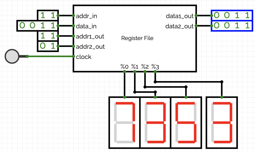
Here's a brief description of how this module can be used:
-
The input addr_in selects a destination register (%0, %1, %2, or %3). When there's a rising edge of the clock signal, the value of data_in is written into this register.
-
addr1_out determines which register content is connected to data1_out and can thus be read.
-
addr2_out determines which register content is connected to data2_out and can thus be read.
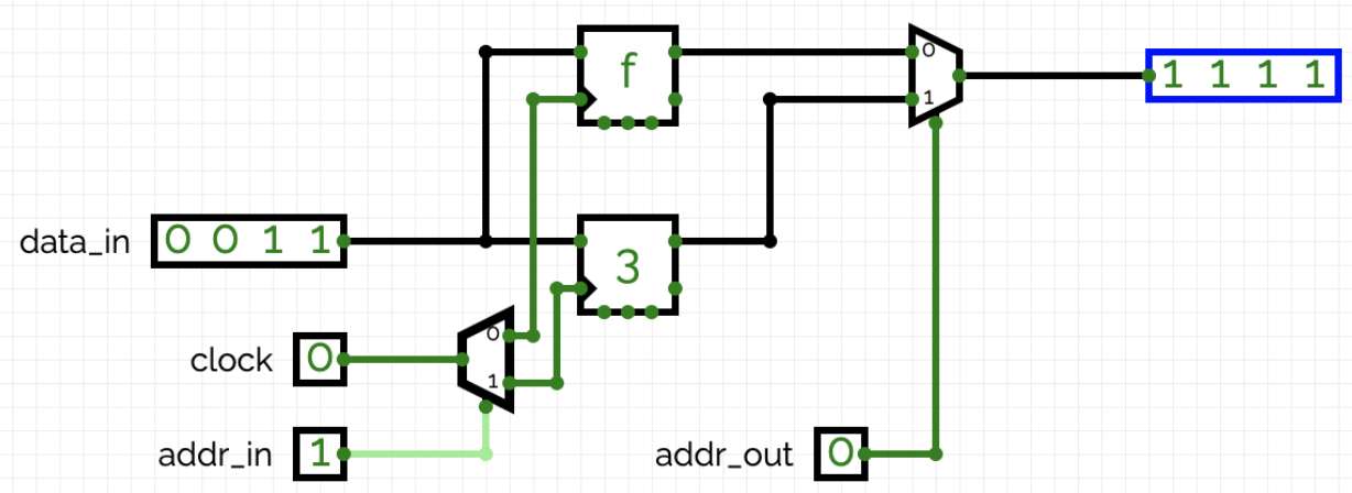
As a guide, here's a circuit showing a register file with two 4-bit registers, where only one register can be read at a time. This demonstrates how multiplexers and demultiplexers can be used in this task: