Crash Course in SystemVerilog: Sequential Logic
In the lecture, we've seen that circuits with flip-flops require consideration of clock signal edges in their mathematical descriptions. This can be achieved by describing a sequence of logical states. For example, with the equations (initial value of ) and (value of after a rising edge), the following circuit with a flip-flop and an inverter can be described:
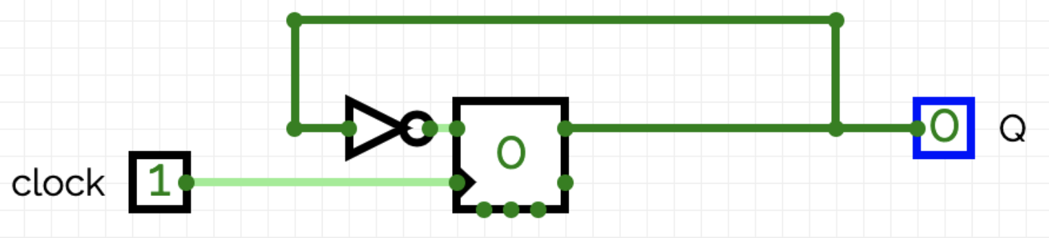
In SystemVerilog, this can be described as follows:
1 2 3 4 5 6 7 8 9 10 11 12 13 14 | module Example3 ( input logic clock, output logic Q ); initial begin Q = 0; end always_ff @ (posedge clock) begin Q <= ~Q; end endmodule |
The initial value is set in the “initial” block, and how the state of Q changes after a rising edge is described in the always_ff block (ff stands for Flip-Flop).
Of course, SystemVerilog allows expressing that a circuit consists of both logic gates and flip-flops, and accordingly, it can be described with both combinatorial and sequential logic. For example, this circuit
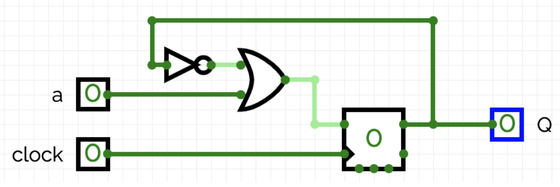
can be described by the following SystemVerilog code:
1 2 3 4 5 6 7 8 9 10 11 12 13 14 15 16 17 18 19 20 21 | module test (
input logic a,
input logic clock,
output logic Q
);
logic nextQ;
initial begin
Q = 0;
end
always_comb begin
nextQ = ~Q | a;
end
always_ff @ (posedge clock) begin
Q <= nextQ;
end
endmodule
|